Реферат: Physical Methods of Speed-Independent Module Design
Реферат: Physical Methods of Speed-Independent Module Design
Oleg Izosimov
INTEC
Ltd, Room 321, 7a Myagi Street, Samara 443093, Russia
1. Introduction
Any method of
logic circuit design is based on using formal models of gates and wires. The
simplest model of a gate is determined by only two "parameters": (a)
Boolean function is to be calculated, (b) fixed propagation delay. The simplest
model of a wire is an ideal medium with zero resistance and consequently, with
zero delay. Such simple models allow circuit design procedures which are a
sequence of elementary steps easily realized by a computer.
When logic
circuits designed by using the simplest models expose unreliable operation as
in the case of gate delay variations, designers introduce less convenient but
more realistic models with arbitrary but finite delay. Using more complicated
models may produce logic circuits that are called speed-independent [1].
In
speed-independent circuits transition duration can be arbitrary. So a centralized
clock cannot be used. Instead special circuitry to detect output validity is
applied. Besides, additional interface circuitry is needed to communicate with
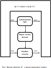
the environment in a handshaking manner. A speed-independent circuit can be
seen as a module consisting of combinational logic (CL) proper, CL output
validity detector (OVD) and interface circuitry (Fig.1). To enable OVD to
distinguish valid output data from invalid ones, the redundant coding scheme
was proposed [2]. The main idea of the scheme is to enumerate all possible
input and output data, both valid and invalid. The OVD must be provided with
appropriate information on data validity. To realize the idea of redundant
coding some constraints on CL design are imposed [3]:
(i) CL must be free
of delay hazards, i.e. CL output data word must not be dependent on the
relative delay of signal paths through CL.
(ii) In changing
between input states, any intermediate or transient states that are passed
through must not be mapped by CL onto valid output states.
When these
constraints were formulated, the circuit designers realised that not every
Boolean description could be implemented in a speed-independent style. Other
approaches to speed-independent module design were needed.
SIM design as
a science has two branches: logical and physical. For a long time physical
branch was overshadowed in spite of its competitiveness. The main properties
of physical approach to SIM design are:
(a) Arbitrary
coding scheme.
(b) Conventional
procedure of operational unit design.
(c) Races of
signals in SIM do not affect on its proper operation.
In this paper
we propose an approach based on the physical nature of transitions in CL. We
believe that each transition is actually a transfer of energy which can be
naturally detected by physical methods.
From the
viewpoint of a radio engineer CL behaves like a radio transmitter. It emits
radio frequencies in the 108-1010Hz band modulated by signals of
106-108Hz.
Obviously, the carrier wave is produced by gate switchings during transitions
in CL. The modulating wave is produced by control schemes (OVD and interface
circuitry) that detect transition completion and inform the environment about
the readiness of CL. OVD is a kind of radio receiver that extracts the
modulation envelope and enhances the received signal. The main properties that
OVD circuit must expose from a radio engineer's point of view are selectivity
and high gain. Since the useful signals can propagate through non-conducting
medium, OVD circuits can be coupled with CL indirectly.
Advances in
semiconductor technology gave birth to two methods of transition detecting
based on two kinds of the information carrying signal, namely electromagnetic
radiation and current consumption. Frequency of the signal produced by
switching logic gates is determined by gate delay.
For instance,
CMOS network of 1-ns gates produces 1-GHz signal, ECL array of 100-ps gates
gives 10-GHz radiation. Logic circuits consisting of 10-ps gates will emit
infra-red radiation. That signal could be easily detected by photosensitive
devices.
2.
Background
Let us have a
closer look at the structure of speed-independent modules (SIM) as presented in
Fig.1. All input data are processed in CL, all output data are obtained from
CL, too. So, CL is the only unit in SIM which is involved in proper data
processing. The result of that processing is specified by Boolean functions.
Algorithms for calculating the Boolean function are realised by the internal
structure of CL. Generally, its structure is series-parallel as well as
algorithm implemented.
When n-bit
data word is put into the CL, n or more signal propagation paths (SPPs)
can be activated concurrently. So, one can say that the calculation of a
Boolean function by CL is of parallel nature. On the other hand, each SPP is a
gate chain which processes data in a serial manner. So, calculation in CL is
also of sequential nature.
The OVD
circuit is intended for detecting transient and steady "states" of
CL. If any SPP in CL is still "active", CL is in transient state,
otherwise it is in steady state. Each gate switching results in both logical
and electromagnetic effects on its surrounding medium. The logical effects of
switching has been heavily investigated; we consider physical one.
To provide
speed-independence of the module the OVD and interface circuitry must also work
in a speed-independent mode. This means that any arbitrary but finite
transistor or wire delay cannot impair proper operation of OVD and interface
circuitry.
The interface
circuitry is a mediator between OVD and environment of SIM. It implements any
kind of signalling convention, commonly a two- or four-cycle one [4] based on
request Req and acknowledgement Ack signal using. The interface
circuitry receives the output validity (OV) signal from the OVD circuit,
a Req signal from the environment and transmits an Ack signal to
the environment (Fig.1).
Consider an
algorithm of operation for interface circuitry realizing speed-independent
four-cycle signalling convention (FCSC). In accordance with FCSC the control
signals must go in the following sequence: Req+OV-Ack+Req-Ack- where "+" corresponds to rising the
signal and "-" corresponds to falling the signal. All signals are
assumed to adhere to positive logic. Initially the signals Req and Ack
are low, the signal OV is high. If the environment state changes,
the Req signal rises and transient state of CL occurs (OV-). Upon completion of the
transitions in CL, signal OV rises and the interface circuitry generates
the Ack signal rising. After that the environment produces a falling Req
signal and then the interface circuitry transmits the falling Ack signal
to the environment. All the signals have to be reset into the initial state.
To develop the
interface circuitry a circuit designer must take into account that any OVD
circuit has finite (non-zero) turn-on delay ton.
This means that OVD cannot respond on transitions of short duration t tr< ton .
An example of
interface circuitry is shown in Fig.2. It contains a flip-flop, a NOR-gate, an
asymmetrical delay and an inverter as an output stage [5].
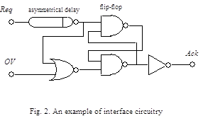
The
asymmetrical delay is intended for delaying Req rising signal for + period
where + > ton .
Delaying Req falling signal noted - is to be as short as possible. Note that speed-independent
operation of interface circuitry is
vulnerable to delay + variation.
If + becomes
less than ton ,
proper operation of SIM can not be guaranteed. Otherwise, if + is
much more than ton ,
performance of SIM will be significantly reduced. To provide exact accordance
of + and ton a
circuit emulator can be used.
Such an
emulator is either an exact copy of OVD or its functional copy, i.e.
resistive-capacitive model of OVD's critical path. In the chip the emulator
must be placed next to active OVD circuit in order to ensure identical
conditions of fabrication and operation.
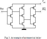
In this
example we use a simplified asymmetrical delay implemented as an asymmetrical
CMOS inverter chain (Fig.3). Contrary to the common inverter an asymmetrical
one has non-equal rise and fall times of output signal.
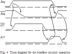
A time diagram
for interface circuitry is presented in Fig.4 for two cases: (a) ttr < ton and
(b) ttr ton.
In case (a) the signal sequence Req+Ack+ is
formed for (++tNOR)
period where tNOR is
a NOR-gate delay. In case (b) the above sequence is formed for (ttr +toff+tNOR)
duration where toff is
a turn-off delay of OVD circuit. When the SIM returns to the initial steady
state, the signal sequence Req-Ack- is formed for (-+tNOR)
interval.
After
considering the SIM in operation it is obvious that the main problems of the
module design are in the area of CL and OVD interaction. This includes (a) kind
of signal used as a carrier of information about CL output validity, and (b)
method of OVD circuit design.
4.
Current consumption detection
Using current
consumption of CMOS CL for output validity detection was proposed in 1990 [7].
Contrary to the method of EMR detection this one is based on introducing direct
coupling of source and receiver. While CL is in steady state it consumes
current of about 10-9-10-8A
which does not allow OVD switching. The interface circuitry gets information on
CL output validity and in turn informs the environment about CL readiness to
input data processing. When an input data arrives CL changes its state to
"transient", current consumption increases to 10-4-10-2A,
which switches the OVD, thus informing the interface circuitry about output
invalidity. The latter lets the environment know about CL business.
After the
computations in the CL are finished, the current consumption decreases down to
the steady state value, and the OVD sends a signal of output validity.
4.1
Information carrying signal
Current
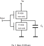
consumption by CMOS CL contains useful information on CL state. CMOS CL is a
network of CMOS gates, so the current consumed by CL is a superposition of
currents consumed by CMOS gates included in the CL. Each CMOS gate contains
PMOS transistor and NMOS transistor networks (Fig.5). While a gate is in a
steady state either the PMOS or the NMOS network is in a conducting mode. When
a gate switches the non-conducting transistor network becomes conducting. There
is usually a short period in switching time when both networks are in a
conducting mode.
Generally,
current consumed by a CMOS gate includes three components [9,10]:
(a) leakage current
Ilk passing
between power supply and ground due to finite resistance of non-conducting
transistor network;
(b) short-circuit
current Isc
flowing while both networks are in a conducting mode;
(c) load
capacitance CL charge current ILC
flowing while a CMOS gate is switching from low to high output voltage via
conducting PMOS network and CL .
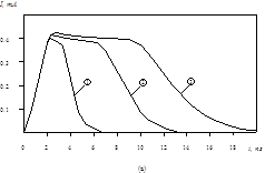
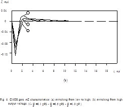
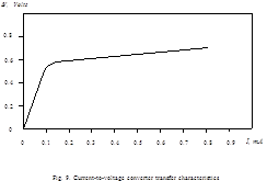
SPICE
simulation has shown [5] that amplitude of current consumed by a typical CMOS
inverter depends on CL and is limited by the non-zero
resistance of the conducting PMOS network (Fig.7). The integral of consumed
current is proportional to CL . When a gate switches from high
to low output voltage, the component ILC is negative by direction and
negligible by value (Fig.7b). It is evident, the switchings from high to low
output voltage occur at the expense of energy accumulated in CL during
the previous switching from low to high output voltage. The component Isc
does not depend on direction in which a gate switches.
The component ILC
equals to ILC
= CLVdd f where Vdd is
a power supply voltage, f is a gate switching frequency. Veendrick has
investigated the component Isc dependencies on CL and
rise-fall time of input potential signal [10]. He showed that if both input and
output signal have the same rise-fall time, the component Isc cannot
be more than 20 percent of summary current consumption [10]. However, when the
output signal rise-fall time is less than input one, the component Isc can
be of the same order of magnitude as ILC. In that case it must be taken
into account. As to the component Ilk, it entirely depends on CMOS
process parameters and for state of the art CMOS devices Ilk is
about 10-15 -10-12 A.
So, the
analysis of CMOS gate current consumption allows us to conclude that in
transient state a CMOS gate consumes a current I= Ilk+Isc+ILC and
in steady state it consumes only Ilk<< I . The difference between two
states from the viewpoint of current consumption is several orders of
magnitude. So, CMOS gate output validity detection is possible, both in
principle and in practice.
In Section 2
we presented series-parallel model of computations in CL. We showed that in
every moment during switching current consumed by CL is a superposition of the
currents consumed on the activated signal propagation paths (SPPs). Now,
considering CL implemented by CMOS devices we should note that while logical
signal propagates through SPP the neighbouring gates switch in opposite
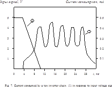
directions. That is why a curve of current consumed by a ten inverter chain
(Fig.8) looks like a combination of crests and troughs. Nevertheless, in the
very lowest point of the curve the current consumed by CL in a transient state
remains several orders more than in a steady state.
4.2
OVD implementation
The proposed
OVD circuit, shown in Fig.9, is a threshold circuit translating an analog
current signal I into a logical signal OV.
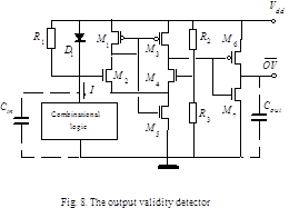
The OVD
circuit contains a current-to-voltage converter (CVC) consisting of the
resistor R1 and
the diode D1.
The OVD also contains a comparator implemented by the MOS transistors M1-M7 and
resistors R2,,,R3 . CMOS
CL consumes the current I and introduces a capacitance Cin . The
capacitance Cout represents
the load caused by the interface circuitry. A low potential output signal of
OVD corresponds to CL output validity. A high potential output signal
corresponds to CL output invalidity. So, OVD generates OV signal in
negative logic manner.
The transfer
characteristics of CVC is determined by a system of three equations:
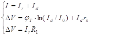 
where I is an input
current of CVC, V is a voltage drop on the
CVC circuit, Ir is
a current flowing through the resistor R1, Id is a
current passing through the diode D1, I0 is a
leakage current of the diode, rb is a bulk resistance of the
diode. Here  stands for kT/q
where k is Boltzmann's constant, T is absolute temperature, q
is charge of an electron. stands for kT/q
where k is Boltzmann's constant, T is absolute temperature, q
is charge of an electron.
Equations
(1)-(3) determine the functional connection F between input current I
and voltage drop V:  . Graphic solution of the
system is shown in Fig.10. . Graphic solution of the
system is shown in Fig.10.
CVC parameters
to be calculated are R1 and rb.
Initial data for calculating R1 are the threshold voltage drop Vth and
corresponding threshold input current Ith . Value Ith is
determined by minimal current consumed by CMOS CL in transient state. Initial
data for calculating rb are maximal voltage drop Vmax and
corresponding maximal input current Imax. Value Imax is
determined by the maximal number of gates in CL switching simultaneously and
their load capacitances.
The comparator
chosen is the CMOS ECL receiver proposed by Chappell et al.[11]. The circuit
includes a single differential amplifier stage with built-in compensation for
parameter variations, followed by a CMOS inverter. The comparator has 100-mV
worst-case sensitivity in 1-m technology. Detailed static and
dynamic analysis of the comparator circuit was given in [11].
The comparator
compares input voltage signal Vin with reference voltage Vref. If Vin <Vref the
comparator output signal equals to logical zero which means that CL outputs
are valid. Otherwise, Vin >Vref, the
comparator output signal equals to logical "one" which means that
the outputs are invalid.
As it follows
from the OVD circuit configuration,
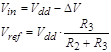 
where
Vdd
is a voltage of power supply.
Equations (4)
and (5) allow us to calculate the threshold voltage drop V of the CVC circuit:
since
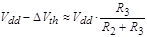 , so , so 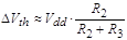 
If 0<V<500mV then the diode D1 of CVC
operates in the very small current region Id 0 and Id <<Ir. So
the component Id
in the Equation (1) can be neglected and IIr =V/R1 .
For practical
values of  the threshold input
current of the OVD circuit is reversely proportional to the resistance of R1 : the threshold input
current of the OVD circuit is reversely proportional to the resistance of R1 :  . Substituting Equation (6)
yields . Substituting Equation (6)
yields
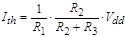 . .
As to choosing
value of rb it must be done with regard to
maximal voltage drop Vmax .
If V>750mV, the diode D1 is in
active mode and while rb <<R1 the
condition Ir <<Id is
true. So, in the large current region IId and
Equation (2) determines an almost linear dependence between I and V. For instance, if the
maximal voltage drop Vmax =900mV
and maximal input current Imax=2mA, then in accordance with
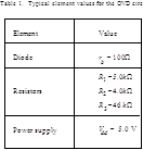
the Equation (2) rb 100. Typical element values for the
OVD circuit with Vth
=400mV are given in Table 1.
The turn-on ton and
turn-off toff delays
of the OVD circuit depend on the OVD itself and the CMOS CL as well. (Switching
the OVD output from low to high voltage is called "turning-on" and
reverse switching is called "turning-off".)
Consider a
piece of CMOS CL and its interaction with OVD circuit (Fig.11). The piece is an
SPP including N logic gates. Each gate is shown symbolically as a
connection of PMOS and NMOS networks. All the capacitances affecting ton and
toff can
be brought down to three components:
(i) CLi is the load capacitance of the
i-th gate;
(ii) Cpsi is
the power supply bus capacitance associated with the i-th gate;
(iii) Cin is
the input capacitance of the OVD circuit.
Let pi is
a probability of the i-th gate being in the state of high output
potential. In this state the capacitance CLi is
connected with power supply bus through the low channel resistance of turned-on
transistors in PMOS network of the i-th gate. Then equivalent
capacitance Ceq connected
to the OVD circuit input equals
 (7) (7)
where N is a number of
gates in the considered SPP. Here the resistance of conducting PMOS network is
assumed to be negligible.
Equation (7)
is also true for CL including several SPPs. In that case summing must be
carried out for all the gates belonging to CL.
Simulation
shows that ton and
toff are
proportional to the OVD time constant =R1Ceq. It was also obtained that when N>20,
the component under the sign of summation in Equation (7) can be much larger
than the component Cin. Due to voltage drop V the effective power
supply voltage is reduced and CL performance is decreased by about 35 percent
[7].
In order to
make SIM operating faster special attention must be paid to reducing the
capacitance introduced by CL.
4.3 Speed-independent address
bus
The simplest
case of CL is a scheme degenerated into a set of wires called a multi-bit bus.
Let us develop the OVD circuit for such a CL.
Multi-bit bus
consists of several lines. Each line can be considered as a medium for signal
propagating from one end of the chip to another. Delay of signal propagation
through a line depends on several factors:
(a) output
impedance and symmetry of driver circuit;
(b) initial state
of the line: if driver is symmetrical, line switching from high to low voltage
lasts shorter than reverse switching;
(c) electrical
properties of the line as a signal propagation medium (resistance of conducting
layer and capacitances between the line and other wires next to it);
(d) length of the
line;
(e) input impedance
and sensitivity of receiving circuit.
Since
different lines of the bus operate in different conditions (a)-(e), signal
propagation delays are different, too. From the standpoint of environment the
bus behaves like any other more complicated CL.
Asynchronous
RAM designers use a bus transition detector since 1980s [13-15]. Such a
detector is usually based on double-rail address coding and two series
connected transistors for each address bit [15]. One of the transistors
receives the true address signal and the other receives the complementary
address signal of the particular address bit. For any steady state condition
one of the transistors will be turned on and one will be turned off. There
will be a finite rise and fall time during a transition of the address bit. There
is a short time during which both transistors are conducting. The establishment
of the conductive path provides the detection of the address transition. In
the first asynchronous RAMs the output signal of the transition detector is
used for bit line precharging and for enabling/disabling sense amplifiers
and peripheral circuitry.
Self-timed RAM
announced in 1983 [14] used transition detectors not for address transition
only but also for detecting read/write completion and address/bit line precharge
completion as well.
The CMOS
transition detector was invented in 1986 [15]. This circuit is also based on
double-rail coding and uses a pair of series-connected NMOS transistors
(Fig.12). The scheme for n-bit bus control contains n line
transition detectors (LTDs) and n AND-gates. Outputs of AND-gates are
united in node M forming wired OR. The output inverter serves as a
pulse shaper. Capacitors C1 and C2 are
intended to prolong rise time of the LTD output signal (true and
complementary). This is necessary for reliable detection.
The main
drawback of the circuit is speed dependence. One can see that if true and
complementary address bit signal have different propagation delays, the
conducting path via NMOS transistors will never be formed.
Using the OVD
circuit proposed in Section 4.2 as LTD we can avoid this drawback.
Note that
address transmission through the address bus is unidirectional. So to detect
completion of bus transition it is enough to recognize the bus state at the
destination end. For this purpose we modify CL to consist of n lines.
The modification means introducing n LTDs, each actually a CMOS inverter
chain. Each chain contains two inverters loaded with a capacitance (Fig.13). Input
of each LTD is connected with corresponding line of the bus at the destination
end. Power supply pads of all LTDs are connected to the current input of the
same OVD circuit.
The parameters
of the input current signal for the OVD circuit are varied by
(i) value of
capacitances C1
and C2 ;
(ii) dimensions of
MOS transistors M1 -M4 .
Since all
transitions in CL are of the same duration and can be lengthened to be outlast
the OVD turning-on time, we simplify the interface circuitry by disallowing
the asymmetrical delay.
Due to short duration of
normal transition in this CL we must take into account the integral nature of
the sensitivity of the OVD circuit. OVD sensitivity depends on both amplitude
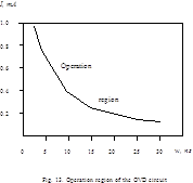
and width of input current pulse. Simulated operation region of the OVD circuit
for current pulses shorter than 30ns is shown in Fig.14. It is obvious that in
this case the threshold of the OVD circuit must be determined by threshold
charge Qth value.
The OVD input charge Q equals to  where
I is OVD input current, t is a moment of time when transition
occurs, w is a width of input current pulse. Turning-on condition for
the OVD circuit is Q=Qth. where
I is OVD input current, t is a moment of time when transition
occurs, w is a width of input current pulse. Turning-on condition for
the OVD circuit is Q=Qth.
When the LTD
circuit shown in Fig.13 is used, the charge value Q is determined by
either C1 or
C2.
Namely, if the line goes from low to high voltage, Q=VC2. If the
line goes in the reverse direction then  where
V is charging/discharging voltage,
approximately equal to the effective power supply voltage: VVdd -V. Here Vdd is OVD
power supply voltage and V is CVC voltage drop. where
V is charging/discharging voltage,
approximately equal to the effective power supply voltage: VVdd -V. Here Vdd is OVD
power supply voltage and V is CVC voltage drop.
The OVD
circuit with typical parameters (See Table 1) has a threshold charge value Qth =4.010-12 C. When C1 =C2 =CL ,
the minimal value of CL providing OVD capacity for
operation is about 1.010-12 F.
Influence of
transistors M1 -M4
dimensions on LTD delay d is determined by approximation [17]:
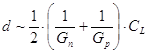
where ~ is a sign
of proportionality, Gn and Gp are
the conductances of NMOS and PMOS transistors respectively (CL =C1 =C2.)
Since  and and  where W and L
are width and length of transistor channels of the corresponding conduction
type, the LTD delay d is proportional to where W and L
are width and length of transistor channels of the corresponding conduction
type, the LTD delay d is proportional to  . .
It has been
obtained that for  , ,  , CL=1.0pF
and Vdd-V=5.0V the LTD delay d=7.6ns. , CL=1.0pF
and Vdd-V=5.0V the LTD delay d=7.6ns.
When LTD works
jointly with the OVD in the speed-independent bus, the real value of the LTD
delay will increase by 30-40 percent due to OVD's R1 effect
on the effective power supply voltage.
To determine
the appropriate value of R1 in the OVD circuit we must know
threshold input current Ith corresponding to threshold
voltage drop Vth recommended
to be equal to 400mV.
Average input
current Iav in
transient state of one line is determined by the expression Iav =CLv where v is the
average rate of increase in the output signal for an inverter included in LTD.
For typical values v=1.0109 Volts per second and CL =1.0pF,
Iav =1.0mA.
Accepting Ith =0.4mA
and Imax=2.0mA
we obtain R1=1k and rb=100.
Simulation has
shown that in this case OVD turning-on delay can be approximated by an
empirical expression:
ton[ns]=8.1+0.1n
where n is the address bus
bit capacity. Total delay of recognizing address transition ttot =dg+ton where
g is a coefficient of the LTD delay increase due to reducing power
supply voltage. As we showed above g1.35. It can be seen that if n=32,
ttot=21.6ns.
4.4 Speed-independent adder
The circuit we
use in this Section as a CL was a touch-stone for many speed-independent
circuit designers for about four decades. We mean a ripple carry adder (RCA)
which is actually a chain of one-bit full adders (Fig.14).
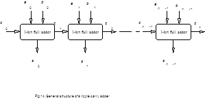
Each full
adder calculates two Boolean functions: sum si=aibici and
output carry ci+1=aibi+bici+aici
where ai,
bi
are summands, ci is
input carry and stands for XOR operation.
In 1955
Gilchrist et al. proposed speed-independent RCA with carry completion signal
[18]. In 1960s that circuit was carefully analyzed and improved [19-21]. In
1980 Seitz used RCA for illustrating his concept of equipotential region and
his approach to self-timed system design [4].
Now we use RCA
as a CL for illustrating our approach to SIM design.
As it was
shown in Section 4.2 the turn-on and turn-off delays of the OVD circuit are
proportional to the equivalent capacitance Ceq associated
with OVD circuit input. Capacitance Ceq depends linearly on a number of
gates N in CMOS CL. To speed up a SIM it is necessary to reduce a number
N. This can be reached by structural decomposition CMOS CL into
subcircuits CL1, CL2, etc. Each subcircuit CLi is connected to its own
detecting circuit OVDi or directly to the power supply if this
subcircuit transition does not affect the transition duration in CL as a whole.
Each detecting circuit OVDi generates its own OV signal which is
combined with other OVDs' output signals via a multi-input OR (NOR) element.
The output signal of that element serves as OV signal of the CMOS CL.
Multi-bit RCA
computation time is determined by length of maximal activated carry chain. A
lot of papers were devoted to analysis of carry generation and carry propagation
in RCA [19-21], many of them contained their own methods for estimation or
calculation of average maximal activated carry chain. We do not intend to add
another one.
Let us have a
look inside RCA. As it was mentioned above RCA consists of one-bit full adders
and each full adder consists of two parts: forming sum si part
and forming carry ci+1 part
(Fig.16).
In multi-bit
RCA all forming sum parts do not interact with each other and do not affect on
transition duration in RCA. Each forming carry ci+1 part
receives ci signal
from preceding forming carry part and sends ci+1 signal
to consequent one.
To decompose
RCA we use three heuristic tricks:
(i) All forming sum
parts we connect directly to power supply.
(ii) We divide each
forming carry part into three subcircuits denoted in Fig.16 by numbers 1,2 and
3. All subcircuits 1 we connect directly to power supply because they do not
contain input ci and
so do not contain carry propagation path.
(iii) All
subcircuits 2 we connect to OVD1 and all subcircuits 3 we connect to OVD2.
Outputs of OVD1 and OVD2 are connected to two-input NOR-gate forming RCA OV
signal in positive logic manner (Fig.17).
OVD1 and OVD2
input currents I1 and
I2 curves
for 6-bit RCA and longest transition duration are shown in Fig.18.
Accepting Vth1,2=400mV
we calculated the OVD circuits parameters. It was obtained R11=5k, Ith1=0.08mA,
R12=3k, Ith2=0.13mA.
OVD1 and OVD2 delay dependencies on a number of bits in RCA are shown in
Fig.19.
4.5 Comparison of SIMs with
synchronous counterparts
Transition
duration in CL is a random variable. Probability of transition with duration D
is determined by implemented Boolean function and distribution of input
logical combinations. Domain of possible values for variable D occupies
the interval [0;Dmax].
Here Dmax is
a length of critical path in CL.
Let  is a mathematical
expectation of transition duration in CL where Di is
a length of i-th SPP in CL, pi is a probability of i-th
path being the longest activated SPP. is a mathematical
expectation of transition duration in CL where Di is
a length of i-th SPP in CL, pi is a probability of i-th
path being the longest activated SPP.
When CL works
in the synchronous mode, the cycle duration Ts is
chosen with regard to maximal transition duration Dmax.
Certain margin must be added to Dmax to provide reliable operation of
CL in the case of CL parameter variations: Ts =kDmax
where k is a margin coefficient.
In SIM cycle
duration is a random variable with expectation Tsi = gDme+toff+tif where
g is a coefficient of CL delay increasing due to reducing power supply
voltage, toff is
turn-off delay of the OVD circuit, tif is an interface circuitry delay.
We determine
efficiency E for speed-independent mode of CL operation as relative
increase of SIM performance in comparison to its synchronous counterpart: . .
Generally,
speed-independent mode is more efficient than synchronous one if Ts >Tsi or,
in other words,  . .
In the case of
RCA 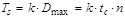 where tc is
a delay of carry forming part, n is a number of full adders in RCA. where tc is
a delay of carry forming part, n is a number of full adders in RCA.
It has been
shown [19] that in n-bit RCA Dme tclog2(5n/4). Then, in the case
of speed-independent operation Tsi=gtclog2(5n/4)+toff+tif.
We have
obtained dependencies of Ts , Tsi on
a number of bits in RCA that are shown in Fig.20. As it can be seen,
speed-independent operation of RCA is more efficient while n>8.
5.Conclusion
6.Acknowledgement
I would like to
thank Igor Shagurin and Vlad Tsylyov of the Moscow Physical Engineering
Institute for helpful discussions of this work. I am also grateful to Chris
Jesshope of University of Surrey and Mark Josephs of Oxford University who
kindly provided the latest material on their research in the area of
delay-insensitive circuit design.
References
[1] Miller, R.E., Switching
theory (Wiley, New York, 1965), vol.2, Chapter 10.
[2] Unger, S.H., Asynchronous
Sequential Switching Circuits (Wiley, New York, 1969).
[3] Armstrong, D.B., A.D.
Friedman, and P.R. Menon, Design of Asynchronous Circuits Assuming Unbounded
Gate Delays, IEEE Trans.on Computers C-18 (12) (1969) 1110-1120.
[4] Seitz, C.L., System
timing, in: C.A. Mead and L.A. Conway, eds., Introduction to VLSI Systems
(Addison-Wesley, New York, 1980), Chapter 7.
[5] Izosimov, O.A., I.I.
Shagurin, and V.V. Tsylyov, Physical approach to CMOS module self-timing, Electronics
Letters 26 (22) (1990) 1835-1836.
[6] Veendrick, H.J.M.,
Short-circuit dissipation of static CMOS circuit and its impact on the
design of buffer circuits, IEEE J. Solid-State Circuits SC-19
(4) (1984) 468-473.
[7] Chappell, B.A, T.I.
Chappell, S.E. Schuster, H.M. Segmuller, J.W. Allan, R.L. Franch, and P.J. Restle,
Fast CMOS ECL receivers with 100-mV worst-case sensitivity, IEEE J.
Solid-State Circuits SC-23 (1)
(1988) 59-67.
[8] Chu, S.T., J. Dikken,
C.D. Hartgring, F.J. List, J.G. Raemaekers, S.A. Bell, B. Walsh, and R.H.W.
Salters, A 25-ns Low-Power Full-CMOS 1-Mbit (128K8) SRAM, IEEE J.
Solid-State Circuits SC-23 (5) (1988)
1078-1084.
[9] Frank, E.H., and R.F.
Sproull, A Self-Timed Static RAM, in: Proc. Third Caltech VLSI Conference
(Springer-Verlag, Berlin, 1983) pp.275-285.
[10] Donoghue, W.J., and G.E.
Noufer, Circuit for address transition detection, US Patent 4563599, 1986.
[11] Huang, J.S.T., and J.W.
Schrankler, Switching characteristics of scaled CMOS circuits at 77K, IEEE
Trans. on Electron Devices ED-34 (1) (1987) 101-106.
[12] Gilchrist, B., J.H.
Pomerene, and S.Y. Wong, Fast Carry Logic for Digital Computers, IRE Trans. on
Electronic Computers EC-4 (4) (1955) 133-136.
[13] Hendrickson, H.C., Fast
High-Accuracy Binary Parallel Addition, IRE Trans. on Electronic Computers
EC-9 (4) (1960) 465-469.
[14] Majerski, S., and M.
Wiweger, NOR-Gate Binary Adder with Carry Completion Detection, IEEE Trans.
on Electronic Computers EC-16 (1) (1967) 90-92.
[15] Reitwiesner, G.W., The
determination of carry propagation length for binary addition, IRE Trans. on
Electronic Computers EC-9 (1) (1960) 35-38.
Appendix
SPICE2G.6: MOSFET model parameters
|
|
|
|
VALUE |
|
|
Name |
Parameter |
Units |
PMOS |
NMOS |
| 1 |
level |
model
index |
- |
3 |
3 |
| 2 |
VTO |
ZERO-BIAS THRESHOLD VOLTAGE |
V |
-1.337 |
1.161 |
| 3 |
KP |
TRANSCONDUCTANCE
PARAMETER
|
A/V2 |
2.310-5 |
4.610-5 |
| 4 |
GAMMA |
BULK THRESHOLD PARAMETER |

|
0.501 |
0.354 |
| 5 |
PHI |
SURFACE POTENTIAL |
V |
0.695 |
0.660 |
| 6 |
RD |
DRAIN OHMIC RESISTANCE |
OHM |
333 |
85 |
| 7 |
RS |
SOURCE OHMIC RESISTANCE |
OHM |
333 |
85 |
| 8 |
CBD |
ZERO-BIAS B-D JUNCTION
CAPACITANCE
|
F |
1.9810-14 |
6.910-15 |
| 9 |
CBS |
ZERO-BIAS B-S JUNCTION
CAPACITANCE
|
F |
1.9810-14 |
6.910-15 |
| 10 |
IS |
BULK JUNCTION SATURATION
CURRENT
|
A |
3.4710-15 |
9.2210-15 |
| 11 |
PB |
BULK JUNCTION POTENTIAL |
V |
0.8 |
0.8 |
| 12 |
CGSO |
GATE-SOURCE OVERLAP CAPACI-
TANCE PER METER CHANNEL WIDTH
|
F/M |
6.7010-10 |
3.3010-10 |
| 13 |
CGDO |
GATE-DRAIN OVERLAP CAPACI-
TANCE PER METER CHANNEL WIDTH
|
F/M |
6.7010-10 |
3.3010-10 |
| 14 |
CGBO |
GATE-BULK OVERLAP CAPACITANCE
PER METER CHANNEL LENGTH
|
F/M |
1.9010-9 |
2.6010-9 |
| 15 |
RSH |
DRAIN AND SOURCE DIFFUSION
SHEET RESISTANCE
|
OHM/SQ |
55 |
30 |
| 16 |
CJ |
ZERO-BIAS BULK JUNCTION BOTTOM
CAPACITANCE PER SQ METER OF
JUNCTION AREA
|
F/M2 |
3.5310-4 |
1.2410-4 |
| 17 |
MJ |
BULK JUNCTION BOTTOM GRADING
COEFFICIENT
|
- |
0.5 |
0.5 |
| 18 |
CJSW |
ZERO-BIAS BULK JUNCTION SIDE-
WALL CAPACITANCE PER METER OF
JUNCTION PERIMETER
|
F/M |
1.7110-10 |
3.2010-11 |
|
|
|
|
|
|
|
|
|
|
|
|
|
|
|